NVIDIA H100 GPUs are actually out there on Paperspace, providing high-performance computing for AI purposes. With a wide array of high-performance GPU machines and a user-friendly platform, Paperspace offers quick access to NVIDIA H100 GPUs.
Join entry to H100 GPUs right here
The Hopper microarchitecture is Nvidia’s newest launch era of GPUs. Every successive model of those Nvidia microarchitectures has include considerably improved bandwidth, VRAM capability, and variety of CUDA cores in comparison with earlier variations. Whereas the highly effective Ampere GPUs, particularly the A100, have introduced in regards to the AI revolution over the previous two years, the Hopper GPU might be anticipated to take this improvement velocity to even increased and sooner ranges than earlier than. This text will discover Ampere and Hopper architectures and canopy the distinction between A100 and H100 GPUs.
Fast Phrases Earlier than Getting Began
Tensor Cores are a sort of processor core present in sure NVIDIA graphics playing cards. The graphics playing cards can carry out calculations extra shortly and with better vitality effectivity with these cores. It helps speed up deep studying and AI workloads, comparable to matrix operations. It makes them significantly well-suited for duties like coaching LLMs.
These are the processor cores present in NVIDIA graphics playing cards. They’re designed to deal with the calculations generally utilized in parallel computing duties and different graphics rendering.
NVLink is a high-speed, direct GPU-to-GPU communication hyperlink. As an illustration, in a multi-GPU setup for advanced simulations or AI mannequin coaching, NVLink permits sooner information switch between GPUs.
NVSwitch is sort of a community change that permits a number of GPUs to speak concurrently at excessive speeds. GPUs can share information quickly and effectively.
This method integrates NVSwitch and NVLink applied sciences for connecting a number of GPUs in a large-scale setup. The aim is to maximise the information throughput and minimise latency in multi-GPU configurations. As an illustration, NVIDIA’s DGX programs have an NVLink Change System that permits high-speed connections between all GPUs within the system.
About NVIDIA Ampere
Ampere GPUs, launched in 2020, marked a major leap ahead in efficiency and energy effectivity. One of many key enhancements was the second-generation RTX applied sciences, which revolutionized real-time ray tracing in gaming and content material creation. The Ampere GPUs additionally made important strides in AI processing, due to the inclusion of devoted tensor cores that speed up AI workloads. Moreover, the Ampere structure’s elevated reminiscence bandwidth and improved energy effectivity have made it a favorite amongst builders and lovers. However now we now have the brand new Hopper structure. Let’s study it intimately.
About NVIDIA Hopper
- The NVIDIA Hopper structure makes use of Tensor Core expertise with the Transformer Engine to hurry up AI calculations. The Hopper Tensor Cores can deal with blended FP8 and FP16 precision. Hopper additionally triples the attainable floating-point operations per second (FLOPS) for TF32, FP64, FP16, and INT8 precision over the prior era. Mixed with the Transformer Engine and fourth-generation NVIDIA, NVLink, and Hopper Tensor Cores, they energy an order-of-magnitude speedup on Excessive-Efficiency Computing (HPC) and AI workloads.
- The NVIDIA H100 GPU is a strong information centre GPU that may be partitioned into smaller, remoted cases referred to as Multi-Occasion GPU (MIG) cases. It permits the GPU for use extra effectively for workloads that do not require a full GPU. MIG partitioning offers roughly 3x extra computing capability and practically 2x extra reminiscence bandwidth per GPU occasion.
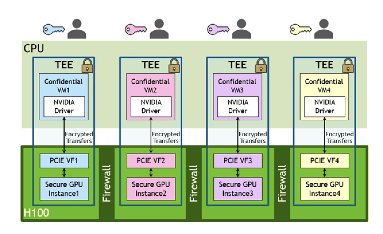
- Confidential Computing is offered to as much as seven particular person GPU cases, every with hardware-based safety features that present confidentiality. Reminiscence isolation is supplied with firewalls. Encrypted transfers happen between CPU and GPU, as proven within the diagram under.
Distinction between Hopper and Ampere Architectures
Expectations from Hopper GPUs
Specifically, the multi-chip module (MCM) design was a extremely anticipated development.
- It permits a number of GPU chips to be built-in right into a single package deal
- It considerably reduces latency and will increase efficiency by enhancing reminiscence bandwidth
- It permits real-time ray tracing for extra real looking graphics rendering. Quicker rendering, improved ray tracing capabilities, enhanced synthetic intelligence (AI) processing, expanded reminiscence capability, and help for the most recent trade requirements might be anticipated
What’s an A100 GPU?
The NVIDIA A100 Tensor Core GPU is a high-performance graphics processing unit designed primarily for high-performance computing (HPC), AI, information centres, and information analytics. GPU reminiscence doubled with the most recent 80 GB A100s and debuted, on the time, the world’s quickest bandwidth at two terabytes per second (TB/s). This GPU might be partitioned into as many as seven GPU cases. All parts are totally remoted on the {hardware} stage with their cache, high-bandwidth, and compute cores.
What’s an H100 GPU?
“Twenty H100 GPUs can maintain the equal of all the world’s web visitors, making it attainable for purchasers to ship superior recommender programs and huge language fashions operating inference on information in real-time”, NVIDIA says
NVIDIA H100 is the brand new engine of the world’s AI infrastructure that enterprises use to speed up their AI-driven companies. The primary product based mostly on Hopper is the H100, which incorporates 80 billion transistors and delivers three to 6 occasions extra efficiency than the Ampere-based A100. It additionally helps an ultra-high bandwidth of over 2TB/, quickens networks 6x the earlier model, and has extraordinarily low latency between two H100 connections. Additionally, the H100 boasts 16896 CUDA Cores. So, it may well carry out matrix calculations sooner than an A100 GPU.
In line with NVIDIA, H100 is about 3.5 occasions sooner for 16-bit inference, and for 16-bit coaching, H100 is about 2.3 occasions sooner. Learn extra about H100 GPU.
💡
Paperspace is devoted to offering next-gen GPUs for next-gen AI purposes. So keep tuned!!
Distinction between A100 and H100 GPU
bandwidth for H100 is inaccurate – 80 GB
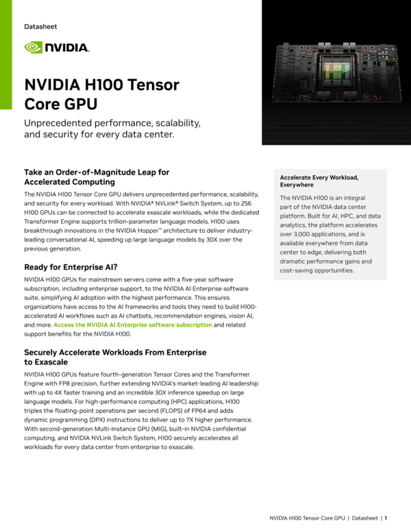
NVIDIA H100 Tensor Core GPU Datasheet
This datasheet particulars the efficiency and product specs of the NVIDIA H100 Tensor Core GPU. It additionally explains the technological breakthroughs of the NVIDIA Hopper structure.
NVIDIA H100 vs A100: Unraveling the Battle of GPU Titans
Find out about two of NVIDIA’s strongest GPUs, NVIDA H100 vs the A100, and see which one is finest to your computing wants.
H100 within the Information
We’ve seen the H100 proliferate within the AI market during the last yr. Listed here are some helpful and related info in regards to the H100’s success with AI coaching.
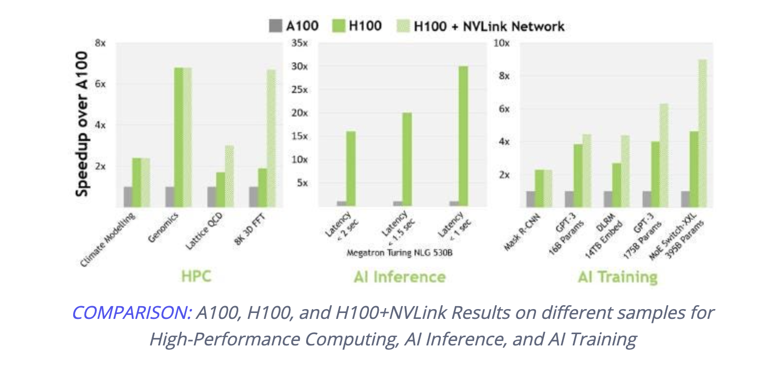
- When coaching the Combination of Specialists Transformer mannequin with 395 billion parameters on 8,000 GPUs, Nvidia mentioned relatively than taking seven days utilizing A100s, coaching on H100s takes solely 20 hours.-NVIDIA
- H100 is the primary GPU to help PCIe Gen5 and the primary to utilise HBM3, enabling 3TB/s of reminiscence bandwidth.-NVIDIA
- The corporate will bundle eight H100 GPUs collectively for its DGX H100 system that may ship 32 petaflops on FP8 workloads, and the brand new DGX.-NVIDIA
- Superpod will hyperlink as much as 32 DGX H100 nodes with a change utilizing fourth-generation NVLink able to 900GBps.-Lambda Labs
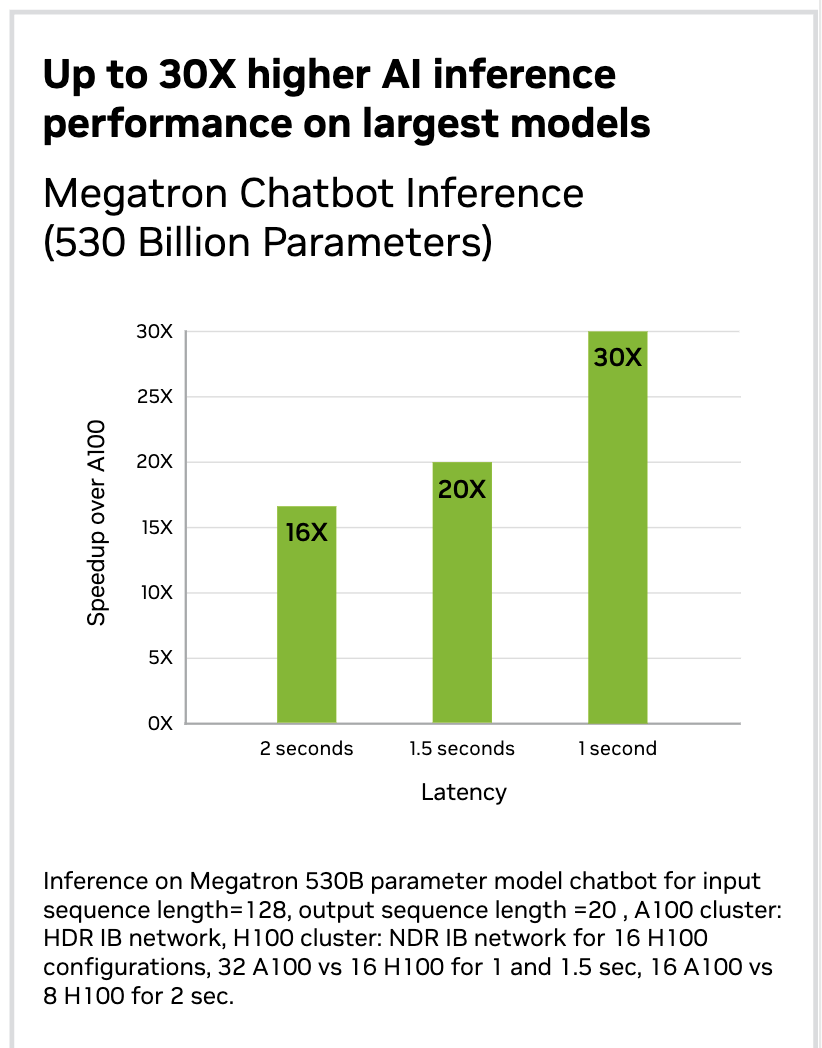
- Nvidia mentioned the H100 may deal with the 105-layer, 530 billion parameter monster mannequin, the Megatron-Turing 530B, with as much as 30 occasions increased throughput.-NVIDIA
When must you use A100 and H100 GPU?
That is fallacious… you make them sound comparable. There isn’t a state of affairs an A100 is outright higher efficiency. The one actual benefit of a100’s are that they’re cheaper.
A100
H100
- H100 is extra geared in direction of scientific analysis and simulations.
- H100 offers high-speed interconnects for workload acceleration.
- It is extra reasonably priced if we’re engaged on a budget-friendly mission. Then it is a sensible choice.
Can the A100 and H100 be used interchangeably?
The reply is typically NO. The A100 and H100 GPUs can’t be used interchangeably. They’ve totally different type components and are designed for various use instances. Notably, the H100 has considerably increased bandwidth and CUDA core counts which allow the H100 to deal with a lot bigger information workloads.
But when we’re nonetheless changing the A100 with an H100, we should contemplate energy and software program necessities. It is strongly recommended to seek the advice of with a GPU knowledgeable or vendor earlier than making any choices. Use this hyperlink to entry and acquire session from our Assist staff.
The way to run H100 GPUs on Paperspace
Closing Ideas
The battle between NVIDIA Hopper and Ampere architectures marks an thrilling time for GPU lovers. Each architectures supply important developments in efficiency, effectivity, and cutting-edge applied sciences. The selection between Ampere and Hopper finally is determined by particular person computing wants and price range constraints. Whereas Ampere GPUs ship excellent efficiency, the upcoming Hopper structure guarantees to push the boundaries even additional. Whether or not we’re content material creators, players, or researchers, NVIDIA GPUs proceed to supply unparalleled capabilities and are price contemplating for the following computing improve.